PCB Prototyping
This page will help you create close to commercial grade single or double sided prototype circuit boards to use with your projects.
I like to design circuits and electronic devices as a hobby, however the most challenging part has always been making a prototype to prove the concept. In particular creating a home made PCB. No matter how good the design was, manufacturing a one-of printed circuit board had always proven to be difficult and time consuming exercise, especially when I had to re-create a PCB because it had flaws and/or was un-acceptable to be used as a prototype. Over the years I have tried numerous methods to create PCBs. Some have worked out well in certain areas and not others. I have used my experience to come up with a sure-fire way to create almost professionally looking PCBs at minimal cost and time
Please follow the few steps below and you will also be able to take the "it's too hard" out of creating an impressive looking prototype.
Blank panels of single or double sided circuit boards come in various sizes. You need to cut out a piece 5mm x 5mm larger than the actual printed artwork ie. 2.5mm extra either side. Please see my Creating PCB Artwork page for hints and guidelines specific to home-made PCBs. I use a band saw to cut the panels to correct shape. Once the panel had been cut to correct shape, both copper surfaces (if double sided board is used) should be sanded with
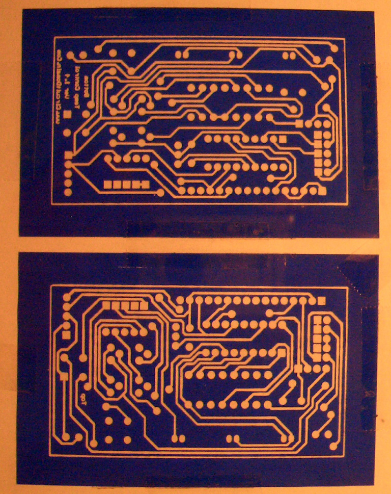
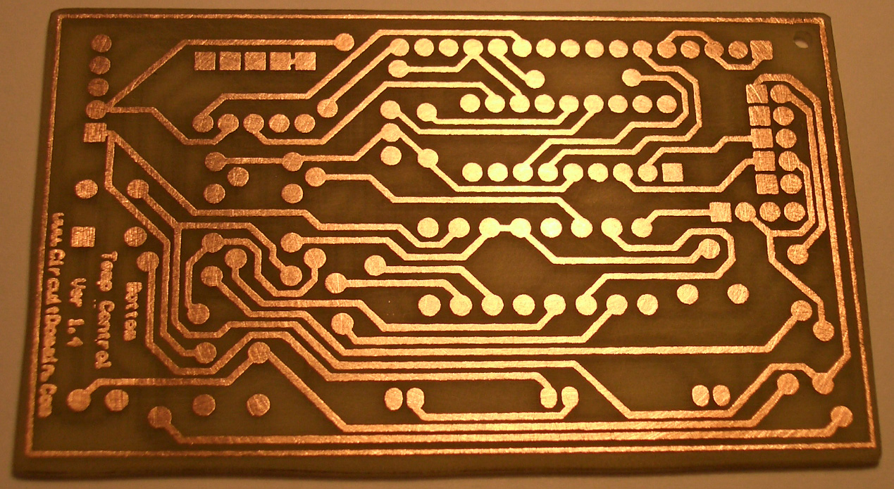
The image to the left shows transfer film after transferring the artwork on to a blank PCB. You can also use Photo printing paper (the glossy type 165 microns) it is much cheaper than film and does the same job. Before you can start you need to print your artwork on to a special transfer film. This film is not too cheap which is more of a reason to get things right the first time. Remember to print Top layer as MIRROR and Bottom layer as is.
The basic preparation for double-sided boards is quiet simple. Cut out the Top and Bottom artwork leaving around 1.5cm on all sides. I must stress that the following step is one of the most important for successful alignment of the two sides of the artwork. Once cut out to correct shape you need to overlay both sides (toner inside, touching) as accurately as you can. When you are happy with the alignment use sticky tape on 3 sides to create an envelope. To make this step easier and more accurate I use sticky tape on one side first and with a sharp
This step is not too difficult but it can be tricky. Once you have prepared a blank panel from STEP 1 and transfer film envelope in STEP 2 you are ready to continue to this step. There are 2 tools you can use.
Tool 1 - A simple clothes iron. This is what I have mostly used (due to the fact that I do not poses a suitable laminator yet) however it is very tricky and with little practice it is possible to transfer on to smaller boards. Larger boards may not align as well as the transfer film and the panel expand when heated up. This coupled with trying to make sure all tracks are heated up may lead to some tracks being broken or over-heated not to mention miss-aligned on far ends of the PCB. To use this method I insert the blank panel in to the envelope making sure it is aligned with the artwork and place the envelope on top of 10 sheets of printer paper (Don't use newspaper or magazines as the heating process will lift the ink from the paper) to make sure I don't damage the table top surface. Set the clothes iron to "Cotton" and wait until it has heated up. Press the iron on to the envelope and hold for 5 seconds to pre-heat the board then lift the iron and slightly tilted (just enough to use the straight edge of the iron) slide the iron edge from one end of the board to the other applying constant pressure (imitating the board going through the heat rollers of a LaserJet printer). 2 or 3 passes should do the trick. Flip the envelope and repeat the process.
Tool 2 - A PCB Fuser. Run the PCB through the PCB Fuser set at 180ºC to 200ºC. Run each side 4 times alternating between sides.
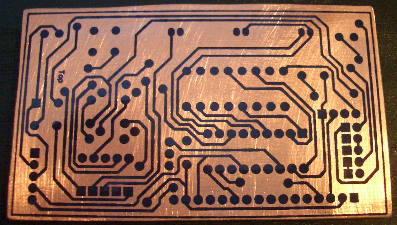
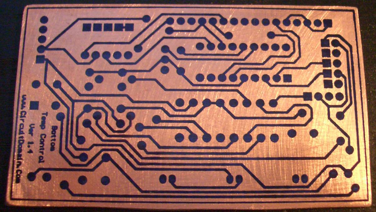
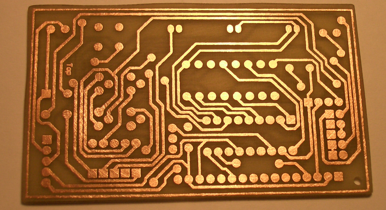
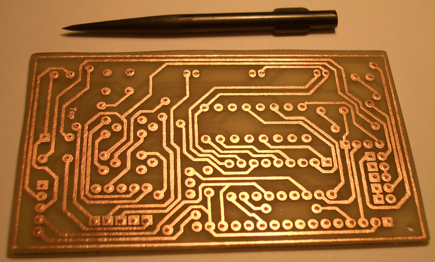
When done both sides, dip the envelope in cold water to cool it down and to soak the paper for 15 min. Cut the sticky tape on all sides with a sharp knife and gently peel off the transfer film or paper. Repeat for the other side. If you have used Photo Paper then you need to rub off under water any white parts on the tracks. Tedious but much cheaper.
Inspect the PCB for breaks in tracks and any shorts. Fix any breaks by touching up with an etch resistant pen. Fix any shorts with a sharp hobby knife. All that is left now is to wash the board in soapy water to get rid of any finger prints from handling.
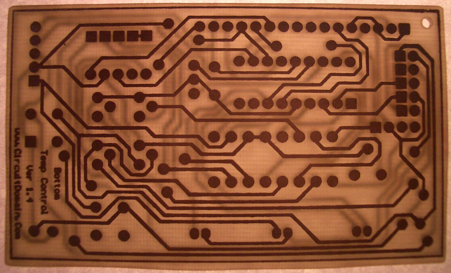
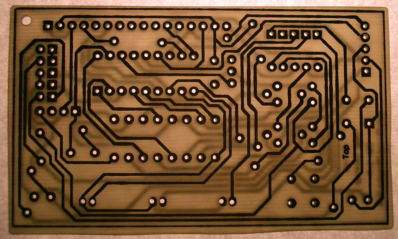
Once the board had been etched, clean it under slow running tap to remove any excess Ferric Chloride. Let it dry and use Acetone or nail polish remover on a cotton bud to quickly remove the toner.
VERY IMPORTANT NOTE: As Ferric Chloride is highly corrosive please follow manufacturers instructions in handling of the chemical and in emergencies. Take every precaution you can.
![]()
Website hosted by WWW.EazySiteHost.Com |